Voltage glitching turns CMP-170HX mining card into an 80 GB A100

A technician used voltage glitching to unlock an NVIDIA CMP-170HX crypto mining card, expanding its VRAM to 80 GB and pushing FP16 performance past that of an authentic A100.
- A technician named Kate used voltage glitching to write to the eFuse controller on an NVIDIA CMP-170HX, which was designed to be read-only.
- Once unlocked, the card reaches up to 80 GB of VRAM, runs over PCIe 4.0, and enables all shader modules. Its FP16 FMA performance surpasses a standard A100 by roughly 20%.
- A 10 GB CMP-170HX sells for around 2500 USD, whereas an 80 GB PCIe A100 can reach 20,000 USD or more.
- Kate reported the vulnerability to NVIDIA, but the company can do little to address cards already on the market.
Table of Contents
From crypto mining card to datacenter GPU
Enthusiasts building local AI rigs now have far more intriguing options than buying a DGX Spark or an Apple Mac Studio. Secondhand datacenter GPUs are widely available, and CMPunlocker software has only accelerated this trend. The soft-mod for the NVIDIA CMP-170HX allows the card to push well beyond its factory limitations.
Now, one technician has taken things a step further. Kate, the creator of the volt-mod, used voltage glitching to bypass the card's remaining constraints. The result is a CMP-170HX that originally packed just 8 GB of VRAM yet outpaces an authentic 80 GB A100 in select workloads.
How the volt-mod works
Kate built upon a research paper describing how to exploit microcode on GA100 cards. She targeted the onboard fuse controller, a component that is normally well-protected. Most CPUs and GPUs feature such a "fuse box." Manufacturers use it only once at the factory to physically disconnect defective chip areas, allowing them to bin and sell the silicon as a lower-tier model.
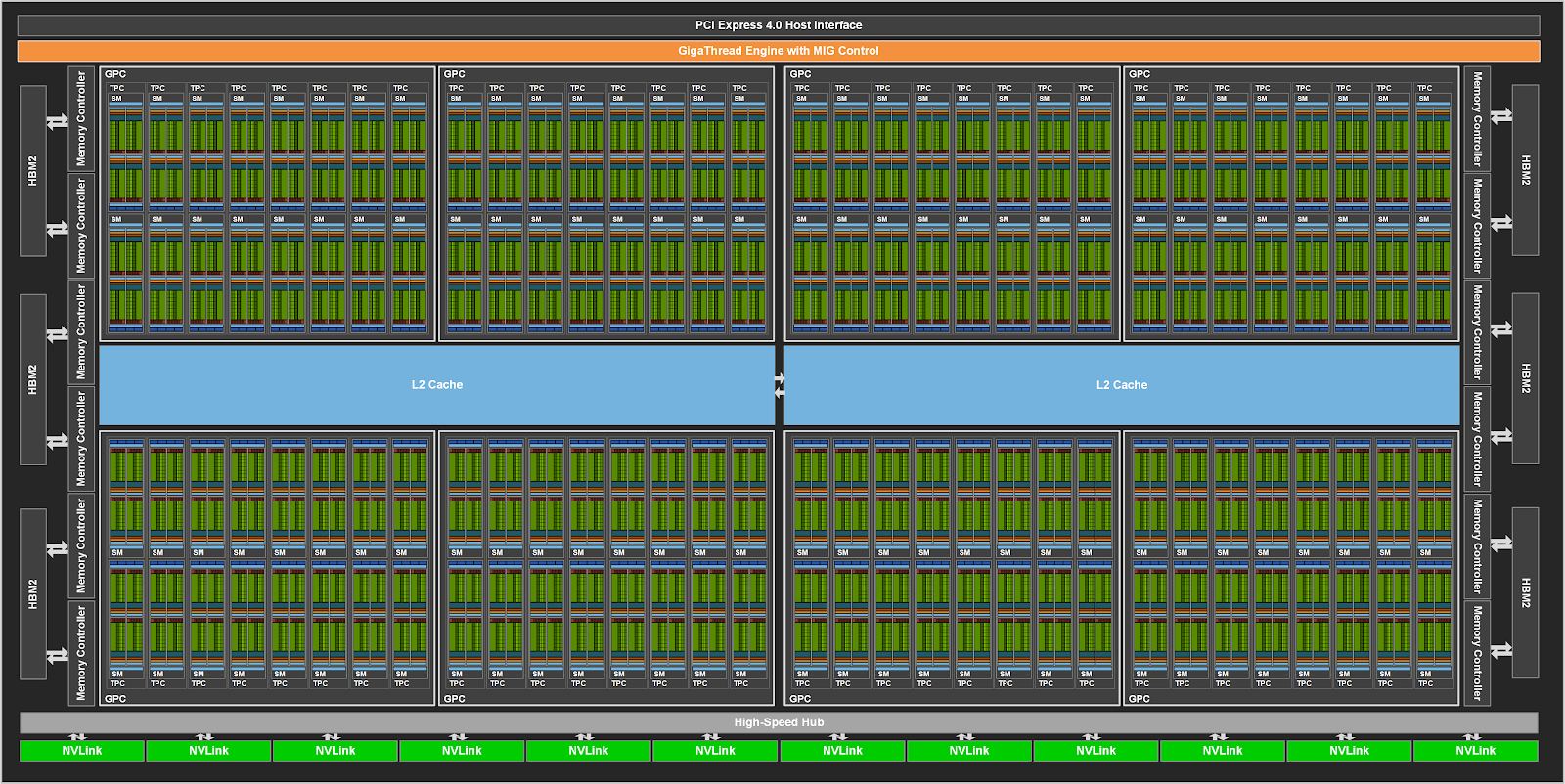
The reason an 8 - 10 GB card can be scaled up to 80 GB is that the GA100 die physically houses the full array of HBM2e stacks. They are disabled at the factory, much like surplus shader modules. The smaller-capacity variant is particularly sought after because it is built on the GA100 revision with 80 GB of HBM2e, whereas the 10 GB card stems from the 40 GB GA100 variant.
The eFuse controller on these cards is quite sophisticated, containing 16,384 bits arranged in a 512 x 32 matrix. Reading this array reveals the card's current hardware configuration. Nearly every part of the GPU maps to corresponding fuses: VRAM partitions, individual shader modules, PCIe 4.0, NVLink, and even hardware video codecs. According to Kate, this design lacks robust security because blowing fuses only enables additional features rather than stripping them away.
Under normal conditions, end users cannot write to these fuses. Kate constructed a modest circuit board around an 8 USD STM32G4 microcontroller to manipulate power signals across the card's PCB. The GPU's VRM controller relies on NVIDIA's PWMVID protocol. Her board intercepts the incoming PWM signals, forcing the VRM to induce voltage transients along the GPU power rail feeding the fuse controller.
By pairing these voltage glitches with rapid, looped reads of the fuse state, she forced the controller into a writable mode. From there, reconfiguring the card became straightforward. She took care to pre-disable shader modules that were originally flagged as defective, since physical fuses cannot be unblown once tripped.
Benchmark results and soft-mod constraints
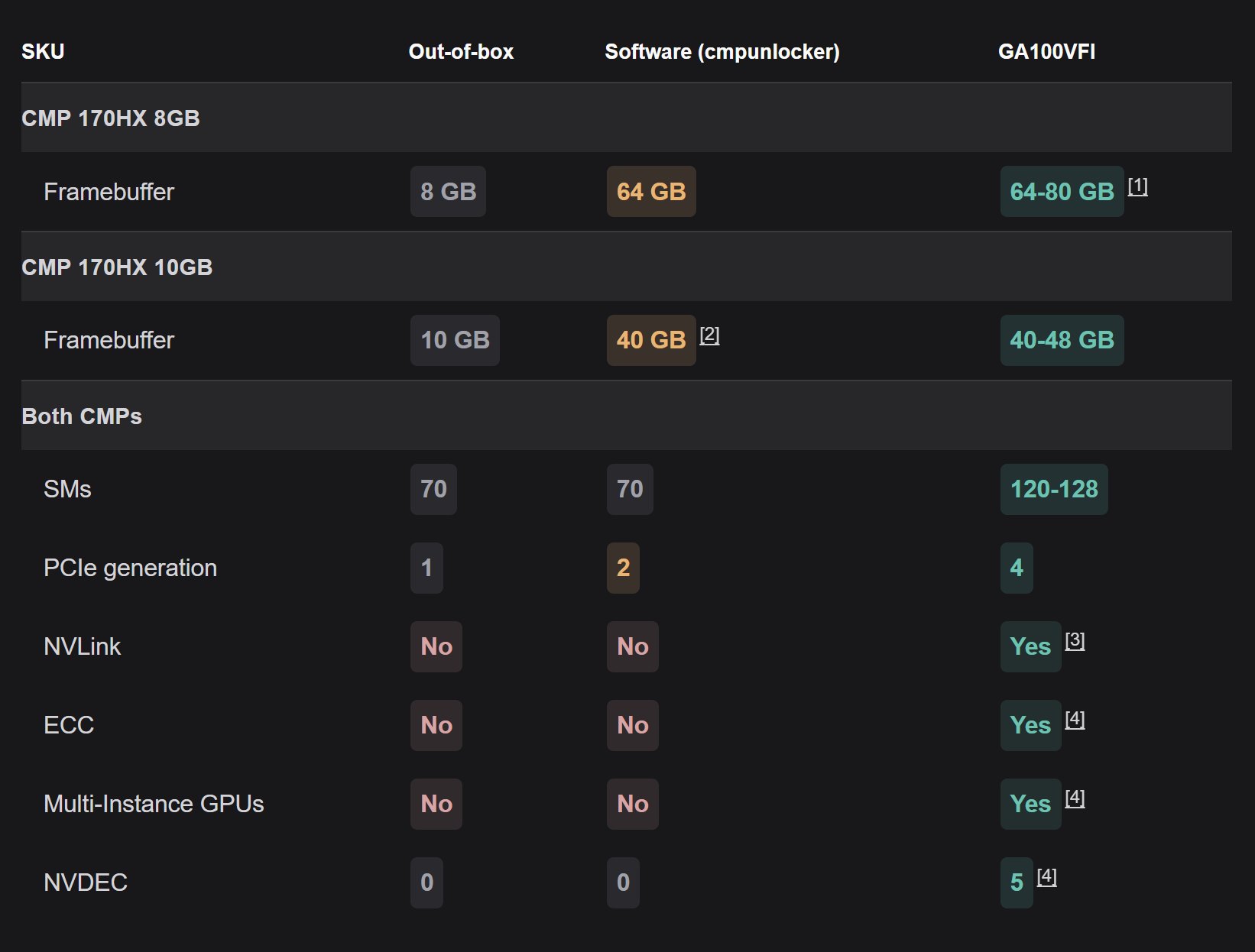
After applying the modification across multiple cards and subjecting them to various benchmarks, Kate confirmed that nine boards operated with the full 80 GB of VRAM. A single card maxed out at 64 GB. Notably, with every shader module (SM) enabled, FP16 FMA performance exceeded that of a standard A100 by roughly 20%. She attributes this gain to the silicon typically having 120 or more functional SMs available - well above the 108 SMs listed in the official specification. The GA100 die inherently packs 128 SMs to offset manufacturing defects, a standard practice across the semiconductor industry.

Meanwhile, CMPUnlocker is still required to expose the "new" features to the driver, though it cannot fully unleash the card on its own. It caps VRAM at 40 - 64 GB depending on the revision, leaves several shader modules locked, and limits PCIe bandwidth to Gen 2 speeds. The card also lacks ECC, NVLink, and multi-instance GPU support - key datacenter capabilities NVIDIA relies on for product segmentation.
Kate's volt-mod strips away every one of these roadblocks. Her best test sample ran reliably at full PCIe 4.0 bandwidth with all features enabled. While she has yet to evaluate the onboard video encoders, few users targeting this class of hardware would care about multimedia encoding.
Pricing and security implications
On the pricing front, the 8 GB CMP-170HX currently commands roughly 3000 USD, while the 10 GB version sits around 2500 USD. A retail PCIe A100 80 GB can climb to 20,000 USD or higher. Server-oriented SXM modules are cheaper, but they demand dedicated enterprise backplanes. These price tags will almost certainly fluctuate once word of this modification spreads throughout the community.
Kate noted that she decided to publish her findings now because another researcher had independently uncovered the same exploit. She disclosed the vulnerability to NVIDIA, though the company can do little to patch silicon that has already reached the open market.
This mod highlights how hardware-level segmentation via fuses can be defeated with inexpensive hardware. Buyers should tread carefully: fuse blowing is an irreversible physical modification, and secondhand prices for older hardware may swing wildly as word spreads. The procedure also demands delicate micro-soldering skills, putting it well out of reach for casual tinkerers.
Nguồn: Tom's Hardware
Reviewed by: Hero Association