
Intel Tech Tour 2025: The 18A era, reshaping AI strategy
Intel presents vision, manufacturing capabilities and technology roadmap at Intel Tech Tour 2025, reaffirming leadership.
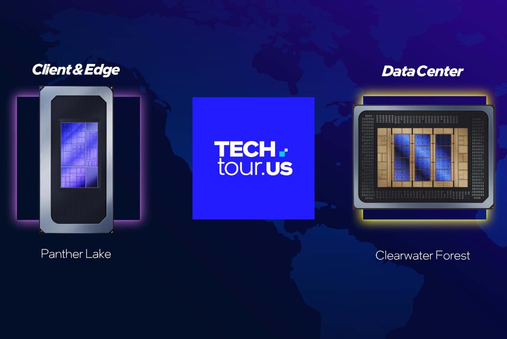
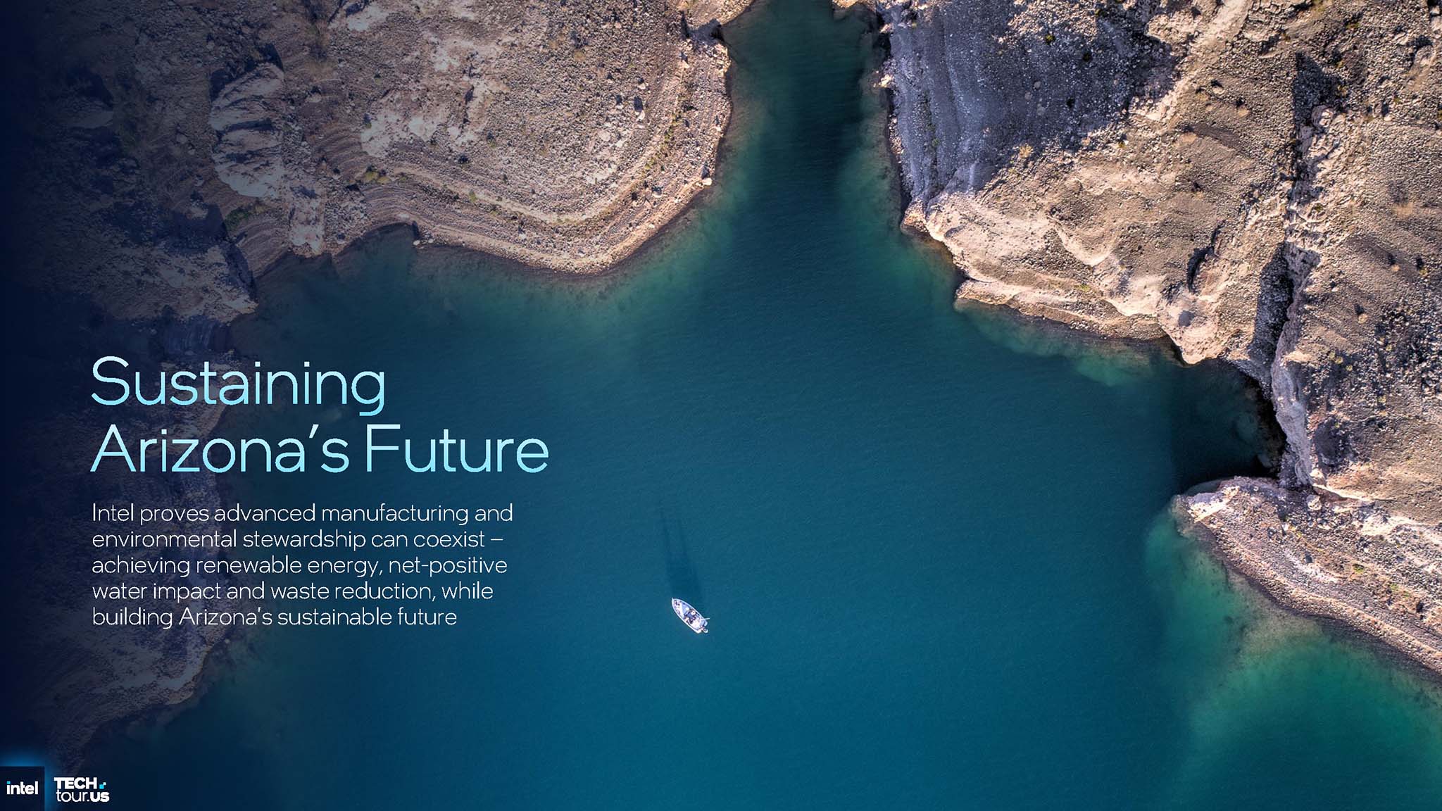
The event took place in Arizona (USA) – an iconic location for Intel. Arizona is home to Fab 52 – the most modern high-volume manufacturing site for the Intel 18A process. Both upcoming strategic product lines, Panther Lake and Clearwater Forest, are built on the Intel 18A process, combined with advanced packaging technology.
Article content
The “New Intel” Vision
The New Intel
Under new leadership, Intel is in the process of restructuring both its culture and its operations. This effort is called “The New Intel”. There are four core pillars to shape the new development phase, shared by Chief Technology Officer (CTO) Sachin Katti:
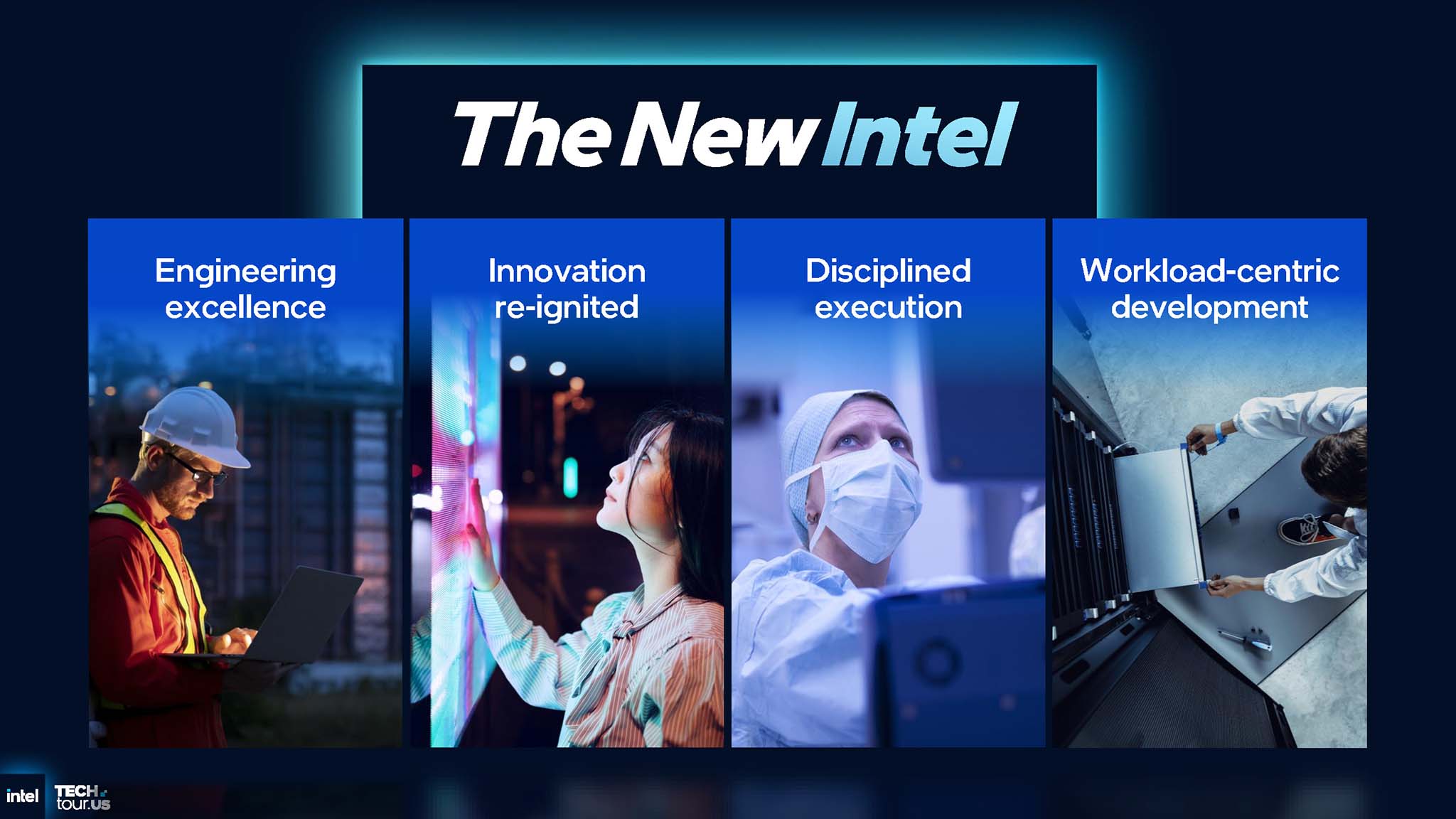
- Engineering excellence: Putting engineers at the center of decision-making.
- Innovation re-ignited: Make selective, disruptive bets across the computing spectrum.
- Disciplined execution: Focus on a few most important priorities and execute them excellently.
- Workload-centric development: Start from real end-customer use cases and work backward to identify the required components, silicon designs, systems and software.
Emphasizing the four principles above is also a tacit admission that Intel has had challenges in the past, as well as delays in roadmaps and execution issues. By reorienting itself to leading engineering goals and putting customer needs at the center, Intel is determined to rebuild trust, have a clear product roadmap and be highly competitive.
The Age of Agentic AI
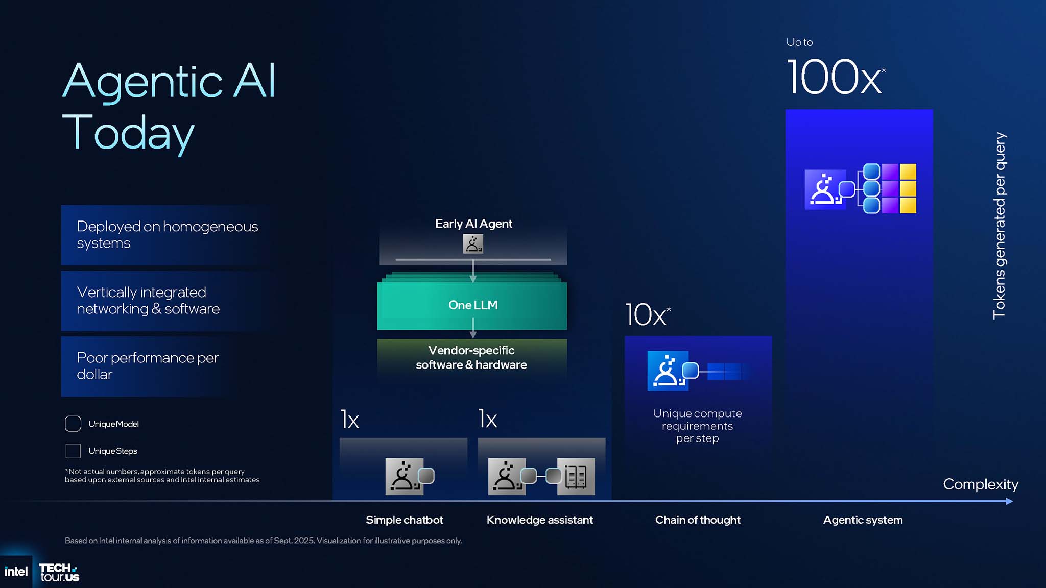
Intel has identified AI as the defining feature of the current generation and will adjust its strategy accordingly. Specifically, Intel will focus on the fastest growing and most valuable segments, which are inference and agentic AI. Agentic AI is defined as AI that has autonomy, beyond the limits of simple response chatbots. Agentic AI becomes systems that can automate complex workflows, interacting with many different models, tools and databases to complete a task.
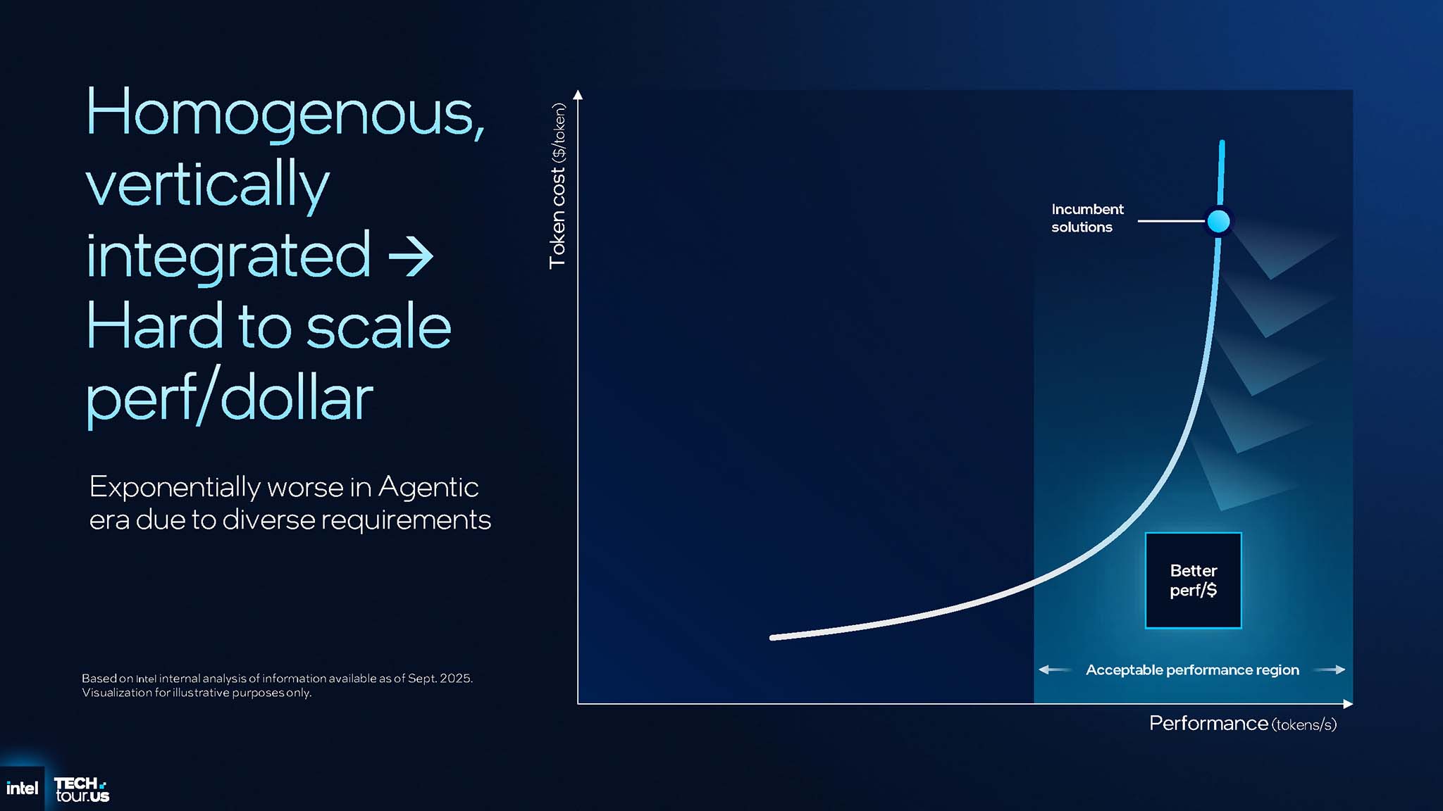
Today’s AI systems are largely built on homogeneous architectures, vertically integrated with proprietary hardware, networks and software. This approach proves to be economically inefficient in the face of the increasing complexity of Agentic AI. To put this in perspective, an Agentic system can generate up to 100 times more tokens than a simple chatbot query, making the operating costs of homogeneous systems difficult to scale. This creates a major barrier to the widespread adoption of AI in businesses and everyday life.
Open, heterogeneous architecture

To address the challenges facing Agentic AI, Intel is introducing a fundamental paradigm shift in AI system architecture. Intel’s vision is that the future of AI infrastructure must be open and heterogeneous. Instead of running the entire task on a single high-end hardware, a heterogeneous architecture separates the components of the Agentic AI pipeline and executes them on separately optimized hardware. For example, the large language model (LLM) prefill stage, which requires a lot of computing power, can run on a GPU optimized for computing, while the decode stage, which requires high memory bandwidth, will run on a memory-optimized accelerator.

However, heterogeneity increases complexity for developers. Understanding this, Intel has built an open software platform – Open AI Software Stack. This platform is designed to abstract the complexity of the underlying hardware, allowing developers to continue using familiar frameworks such as PyTorch and Hugging Face without changing their workflow. The software will automatically analyze, compile and coordinate the components of AI applications onto the most suitable hardware, even on devices from many different vendors.

In early testing, Intel demonstrated the Open AI Software Stack approach. By running the prefill stage of the Llama model on NVIDIA GPUs and the decode stage on Intel accelerators, the heterogeneous system achieved a performance per TCO improvement of up to 1.7x compared to running the entire task on a homogeneous system.
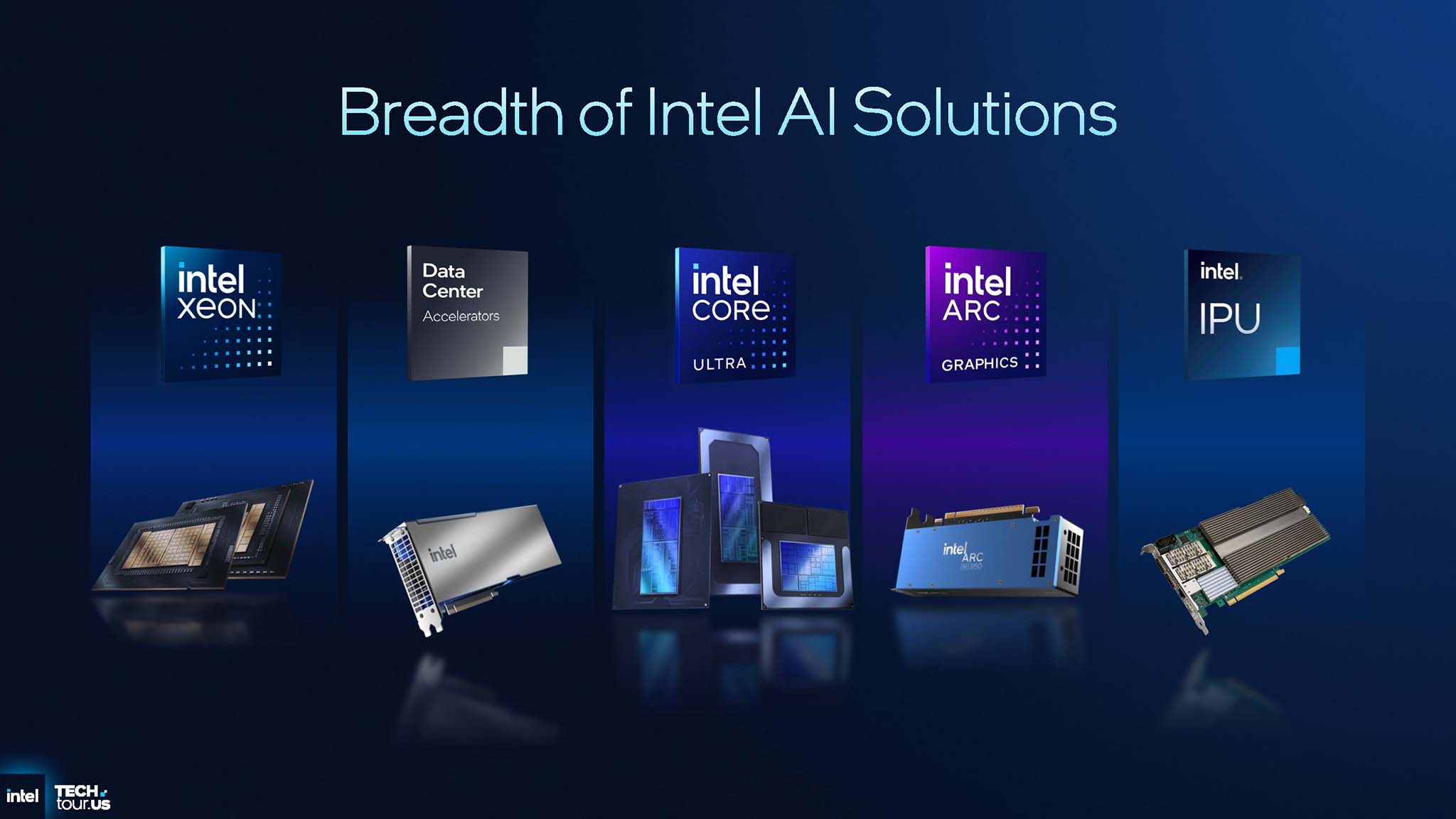
This strategy represents a shift from head-to-head confrontation to selective cooperation and competition. Instead of trying to completely replace NVIDIA’s ecosystem, Intel is creating an open playing field where its products – especially Xeon CPUs – remain an integral part of every AI system. In the long term, the “Open AI Software Stack” serves as a strategic gateway to gradually introduce Intel accelerators into the ecosystem, competing on performance per dollar for specific workloads.
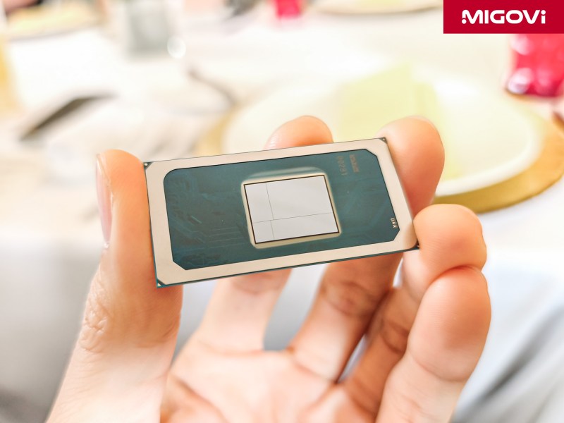
Intel 18A Process
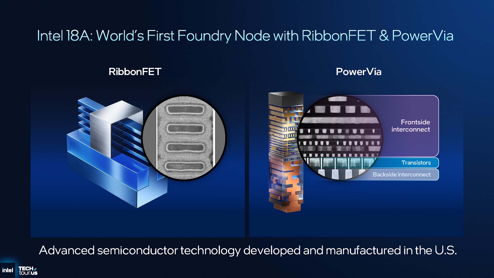
Manufacturing capabilities are the foundation for all of Intel’s future products and strategies. At the event, Intel detailed Intel 18A , the most advanced semiconductor process technology developed and manufactured in the United States and the foundation for Panther Lake and Clearwater Forest. Intel 18A combines two groundbreaking technologies: RibbonFET semiconductors and PowerVia back-side power technology.
Intel Panther Lake technical analysis: CPU, SoC and 18A
Intel Panther Lake Technical Analysis: GPU, NPU and IPU
RibbonFET
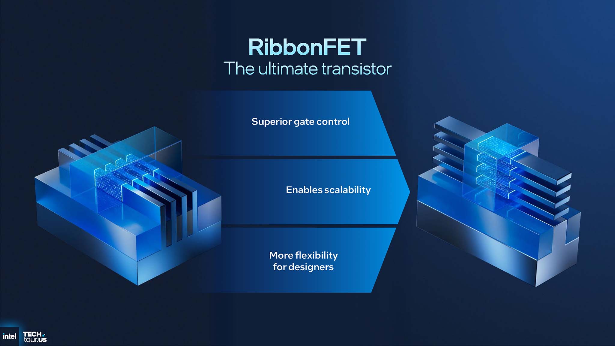
RibbonFET is Intel’s trademark for Gate-All-Around (GAA) semiconductor architecture, which is the next major evolution after FinFET. Instead of the 3-dimensional silicon “fin” structure of FinFET, RibbonFET uses silicon “ribbons” or “sheets” that are completely surrounded by a gate channel on all four sides.
This full encapsulation eliminates the weak point of channel control at the bottom of the FinFET, which significantly reduces leakage current. This not only improves energy efficiency, but also allows designers to continue shrinking the transistor size, which is increasingly difficult with FinFET architectures. Additionally, the width of the “strips” is adjustable, providing greater design flexibility than the discrete fin structure of FinFETs.
PowerVia
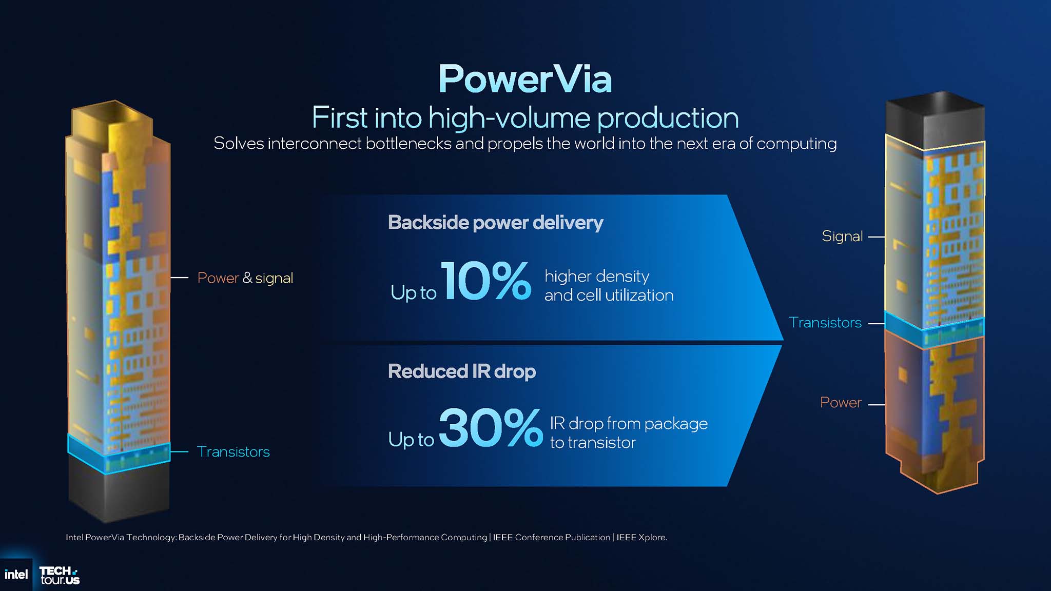
PowerVia is the first backside power delivery technology to enter mass production. PowerVia moves the entire power line network from the front of the wafer to the back of the wafer, leaving the entire front space for signal wires.
Separating the power and signal lines allows for optimization of both. The rear-side power lines can be made larger and thicker to reduce resistance, while the front-side signal lines have more space for more efficient layout, reducing crosstalk. PowerVia increases cell density and utilization by up to 10%, while reducing the IR drop from package to transistor by up to 30%, directly improving performance and energy efficiency.
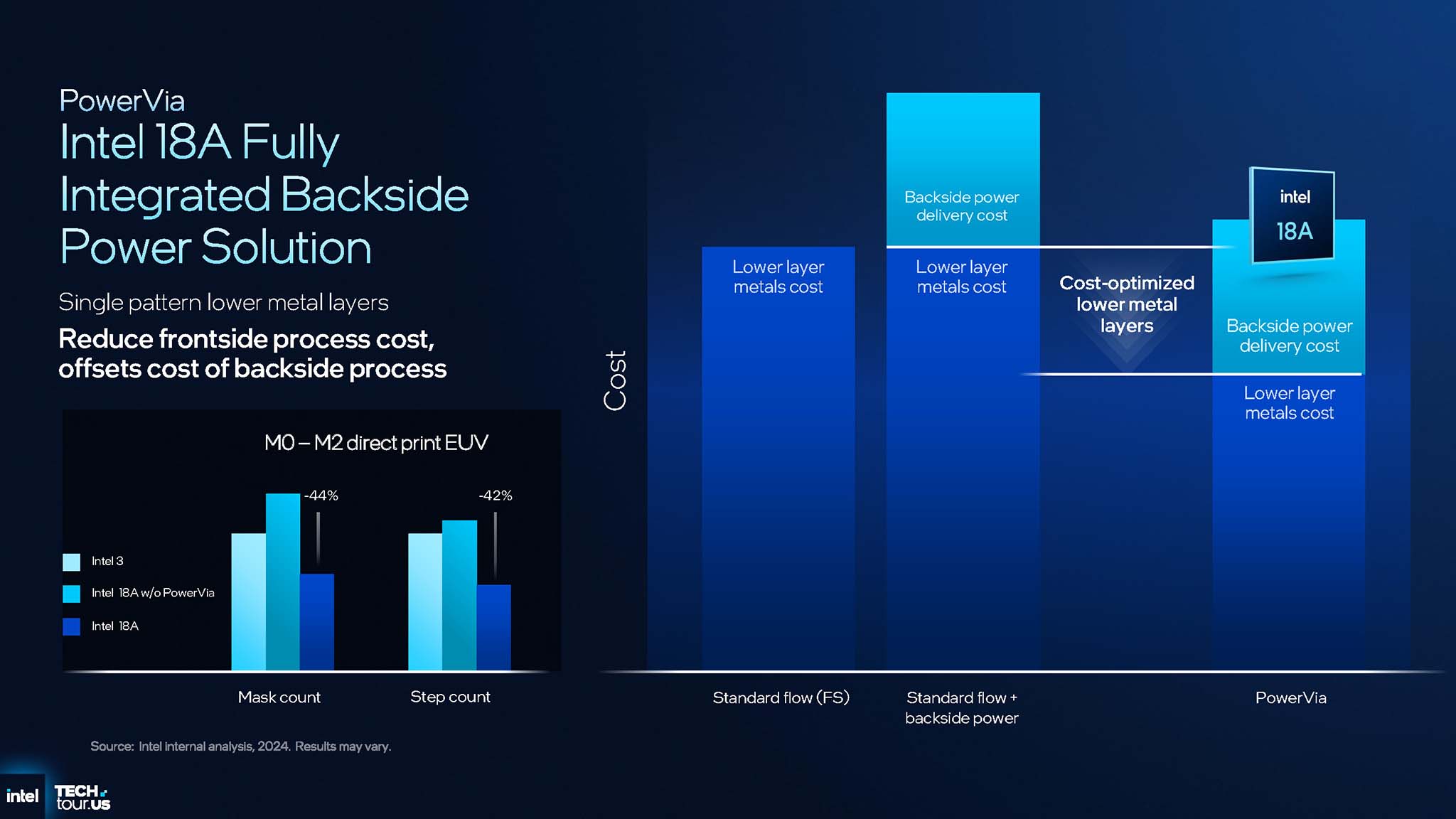
The key aspect of PowerVia is that it is not simply an expensive add-on layer. Intel has optimized the entire manufacturing process for this technology from the beginning. Freeing up space in the first metal interconnect layers (M0-M2) on the front side allows for simpler lithography techniques, which reduce mask counts and process steps by more than 40% compared to the Intel 3 process. These front-side cost savings significantly offset the additional back-side process costs. This shows that PowerVia is part of a comprehensive re-engineering strategy that addresses performance, density and cost issues simultaneously, rather than just a patchwork add-on layer.

Intel confirmed that the 18A process has entered production at two of its US fabs: a development facility in Oregon and the Fab 52 volume production facility in Arizona. Both fabs are in the process of ramping up to volume production.
Intel Xeon 6+ “Clearwater Forest” – A leap forward with Intel 18A and Darkmont
Foveros and EMIB
System on Chip to System of Chips
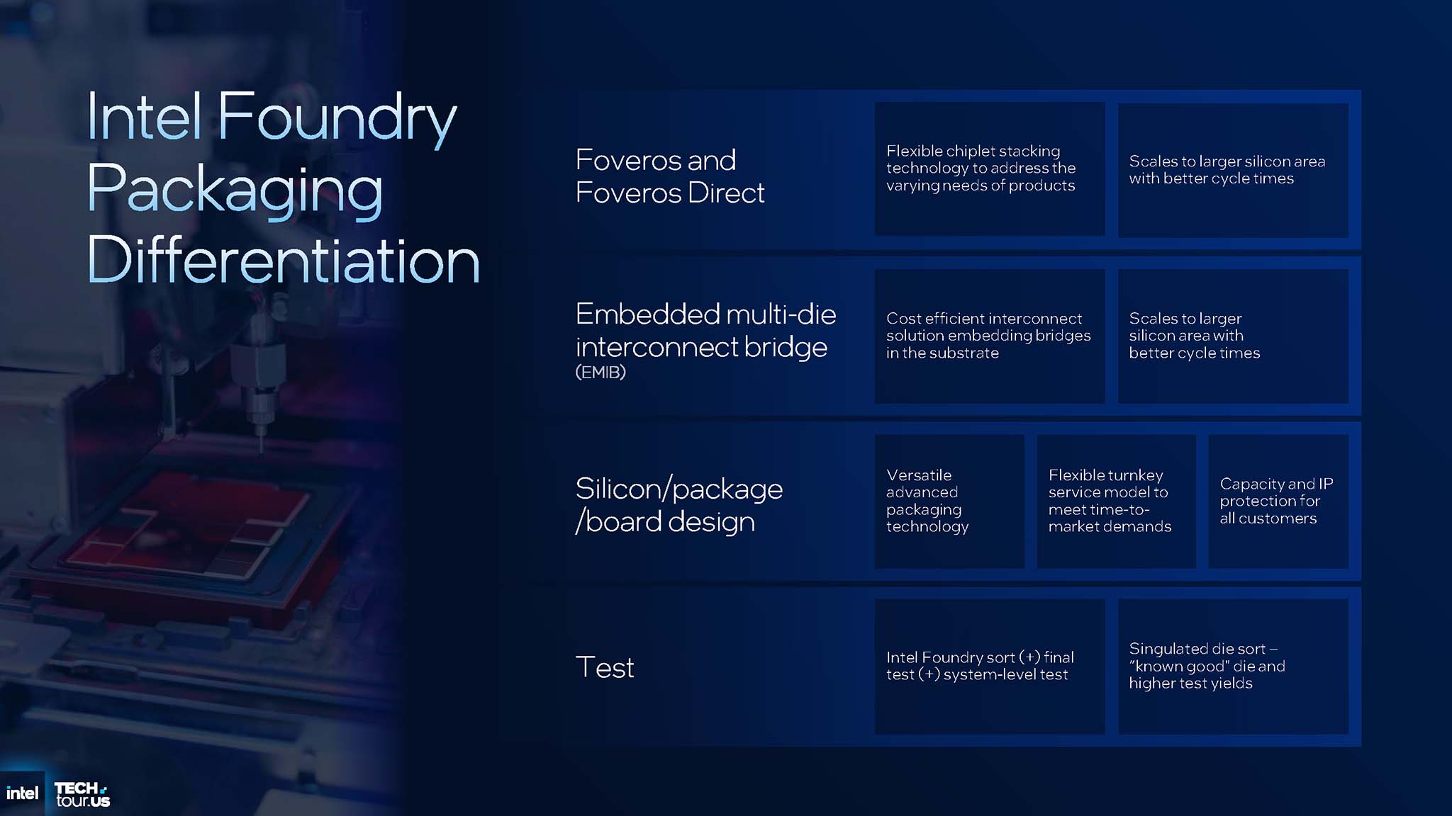
As the AI era is entering its climax, the basic model of monolithic “System on a Chip” (SoC) designs is gradually shifting to a system integrating many chiplets, also called SoC but representing “System of Chips”. The new SoC or System of Chips approach allows the combination of specialized chiplets, manufactured on the most optimized processes for each function, into a single package. This not only overcomes the limitations of reticle size and production yield of large dies, but also brings much better flexibility and scalability. To best meet the new SoC, Intel develops advanced packaging technologies such as Foveros and EMIB.
Packaging technology
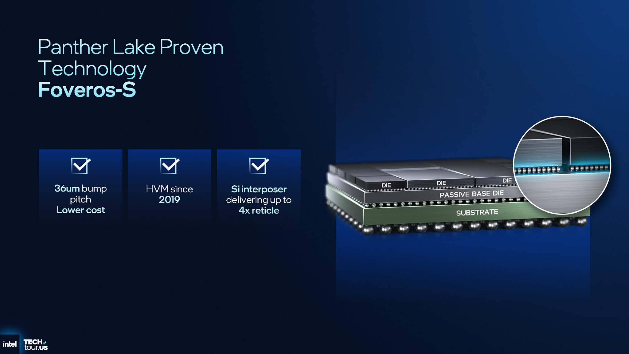
For the next-generation Panther Lake mobile chips, Intel uses Foveros-S packaging technology . This is a solution that has been applied to mass production since 2019. Foveros-S is also the first generation of Foveros, using an intermediate silicon die (silicon interposer), prioritizing the balance between cost, reliability and performance for the high-volume client market. This mature packaging technology has a 36 µm bump pitch, the silicon interposer is capable of connecting dies with a total area of up to 4 times the reticle size. The next variant of Foveros-S is Foveros-R, expected to be ready for production in 2027.
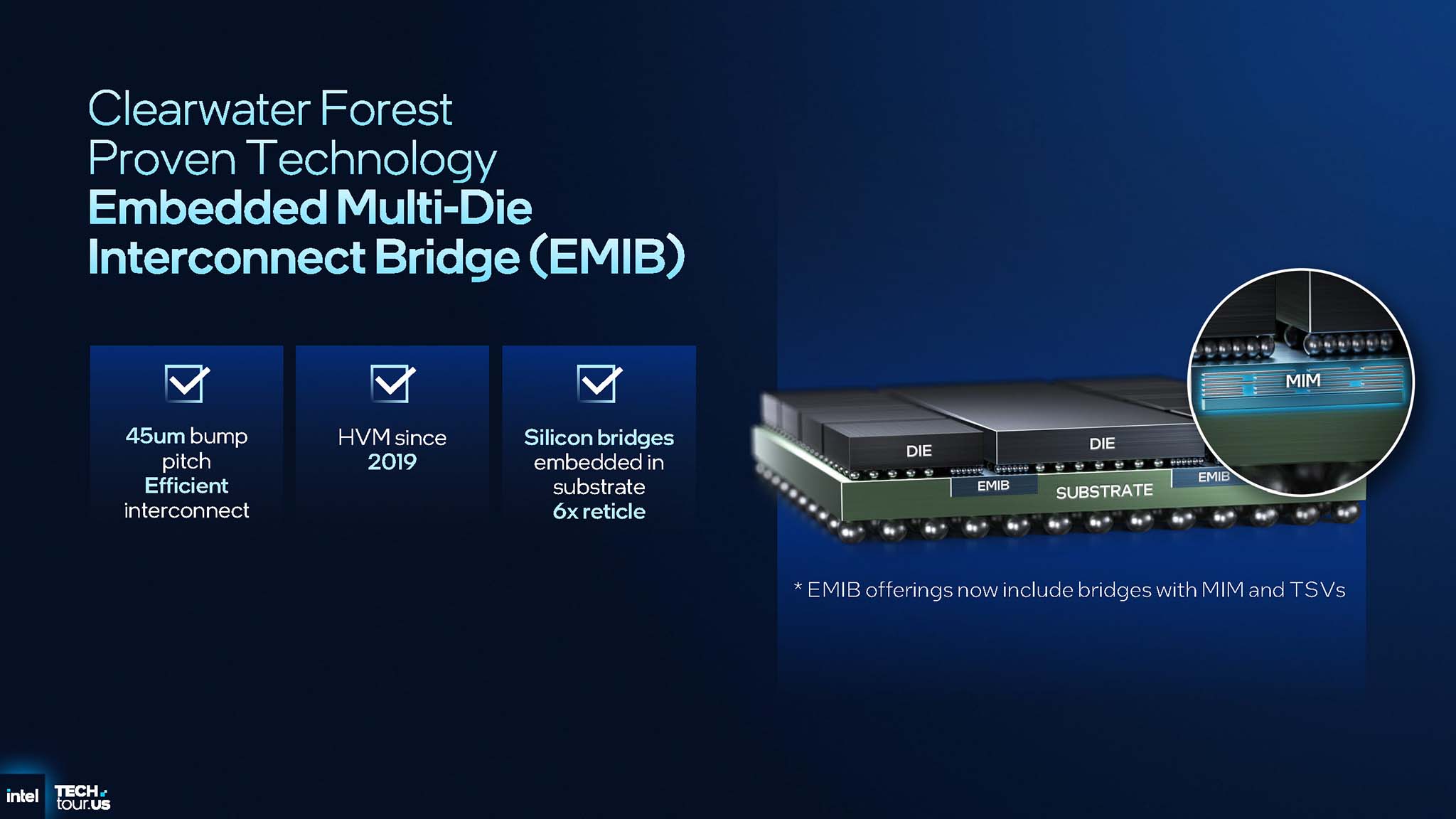
The server market is much more complex with Clearwater Forest, combining two advanced packaging technologies. The first is the third generation EMIB (Embedded Multi-Die Interconnect Bridge), with a 45 µm bump pitch. EMIB uses small silicon bridges embedded directly into the organic substrate to create high-speed die-to-die connections. This is a cost-effective and energy-efficient solution compared to using a large silicon interposer. The technology associated with EMIB is Foveros Direct and Clearwater Forest is also the first product to be mass-produced. Foveros Direct represents a breakthrough in 3D stacking, using Cu-to-Cu hybrid bonding with an ultra-small bump pitch of just 9 µm. The result is the highest density and most energy-efficient die-to-die connections, with an energy consumption of less than 0.05 pJ/bit.
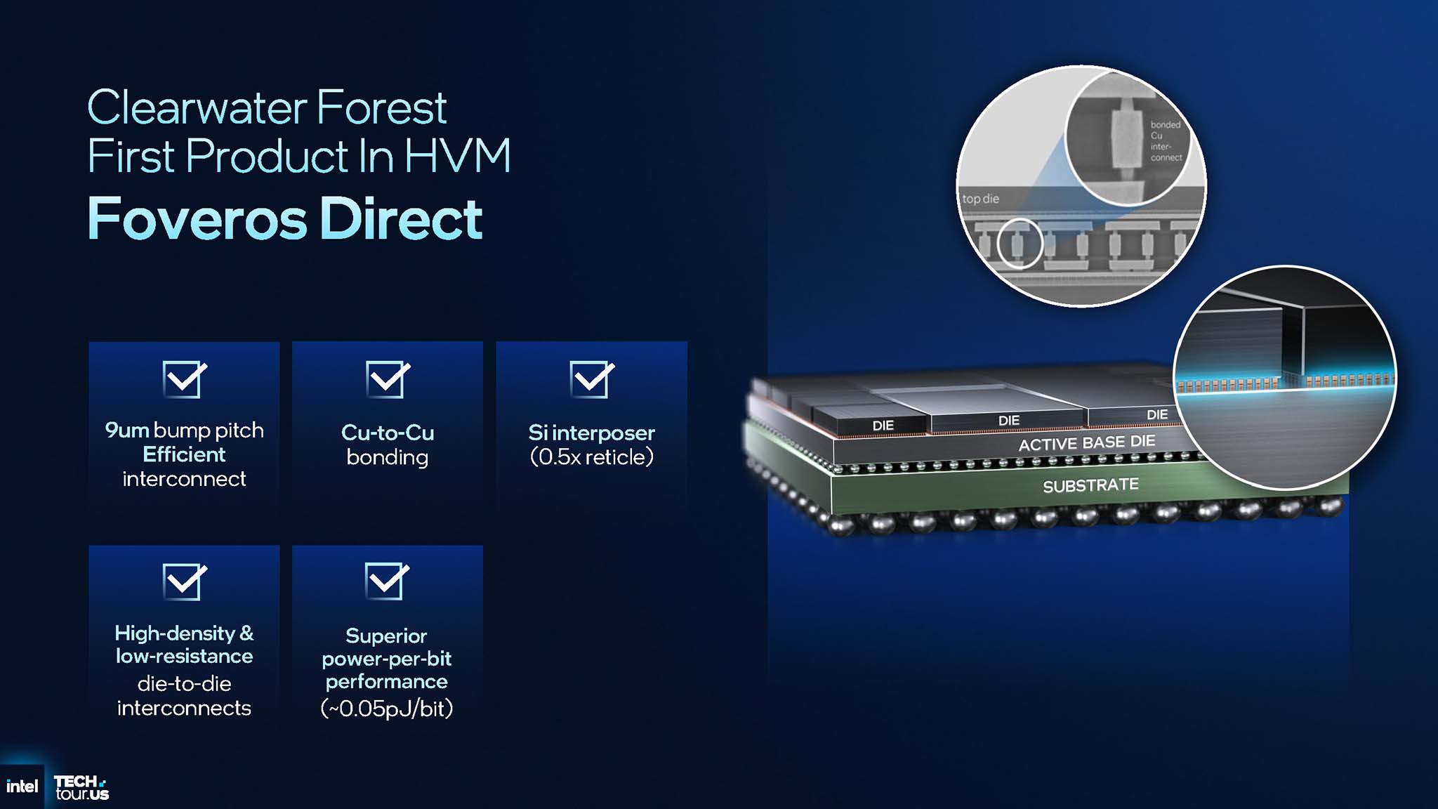
The Clearwater Forest architecture is an extremely complex system, consisting of 12 compute chiplets (manufactured on the 18A process) stacked on 3 base tiles (manufactured on Intel 3) and then connected to 2 I/O tiles (manufactured on Intel 7) via both EMIB and Foveros Direct. Clearwater Forest shows potential customers the capabilities of Intel Foundry, which is able to integrate many chiplets from different processes into a single system.
The Role of Known Good Die
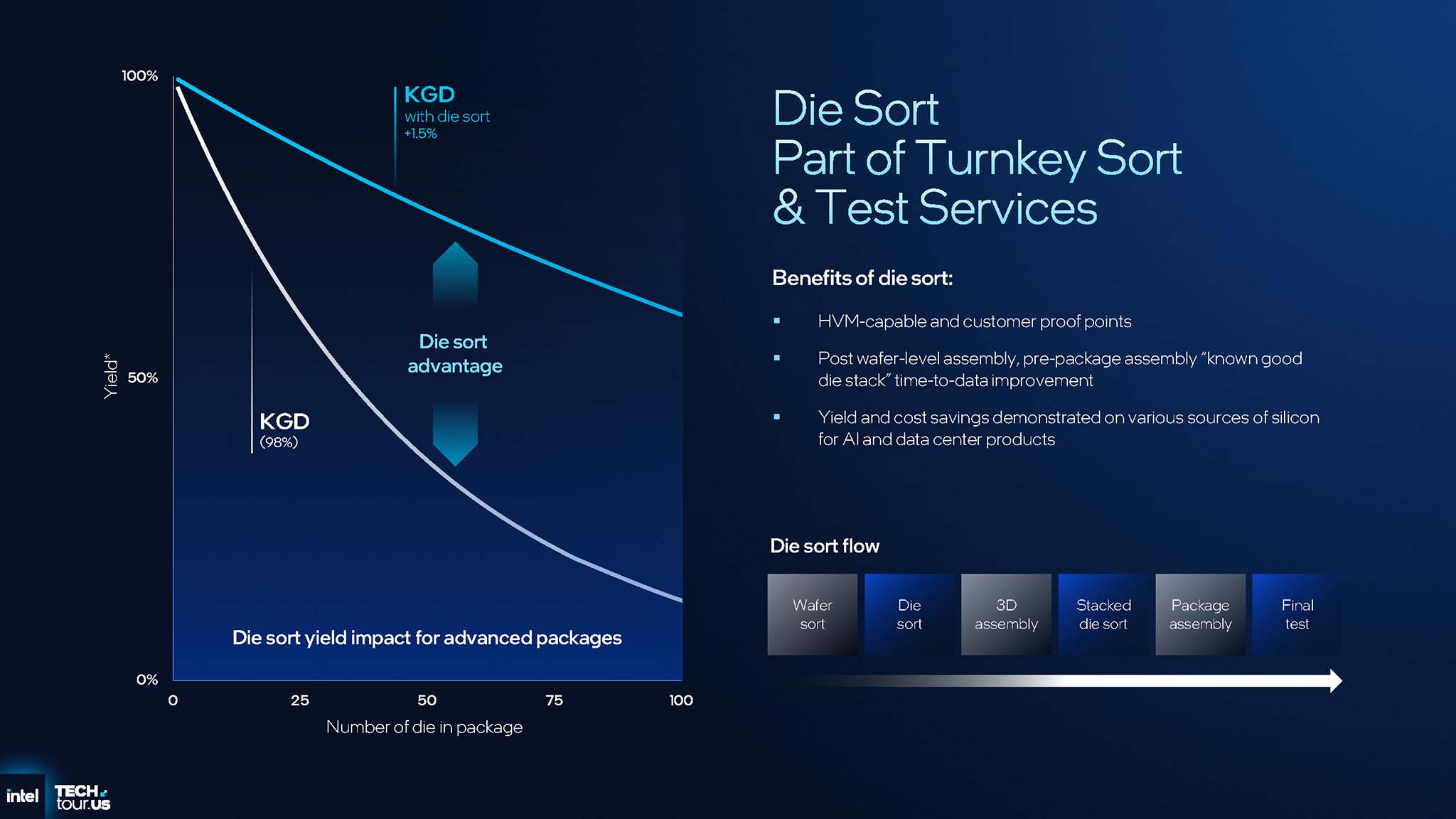
As System of Chips become more complex, Intel’s challenge lies in manufacturing yield. If just one chiplet fails, the entire multi-thousand-dollar package becomes useless. To address this issue, Intel has a KGD (Known Good Die) process. KGD is a comprehensive testing process for single or stacked dies before they are assembled into the final package. The KGD process ensures that only components that have been confirmed to be working perfectly and meet specifications (including power binning) are used. This maximizes final manufacturing yield, reduces scrap costs and brings predictability to a complex manufacturing process like Clearwater Forest.
Beyond the technical test, Known Good Die is the fundamental economic enabler for a multi-chiplet strategy. Intel has invested in state-of-the-art KGD test technology to ensure the profitability of its advanced packaging business. Both Clearwater Forest and Panther Lake now use KGD in manufacturing.
The Importance of Fab 52
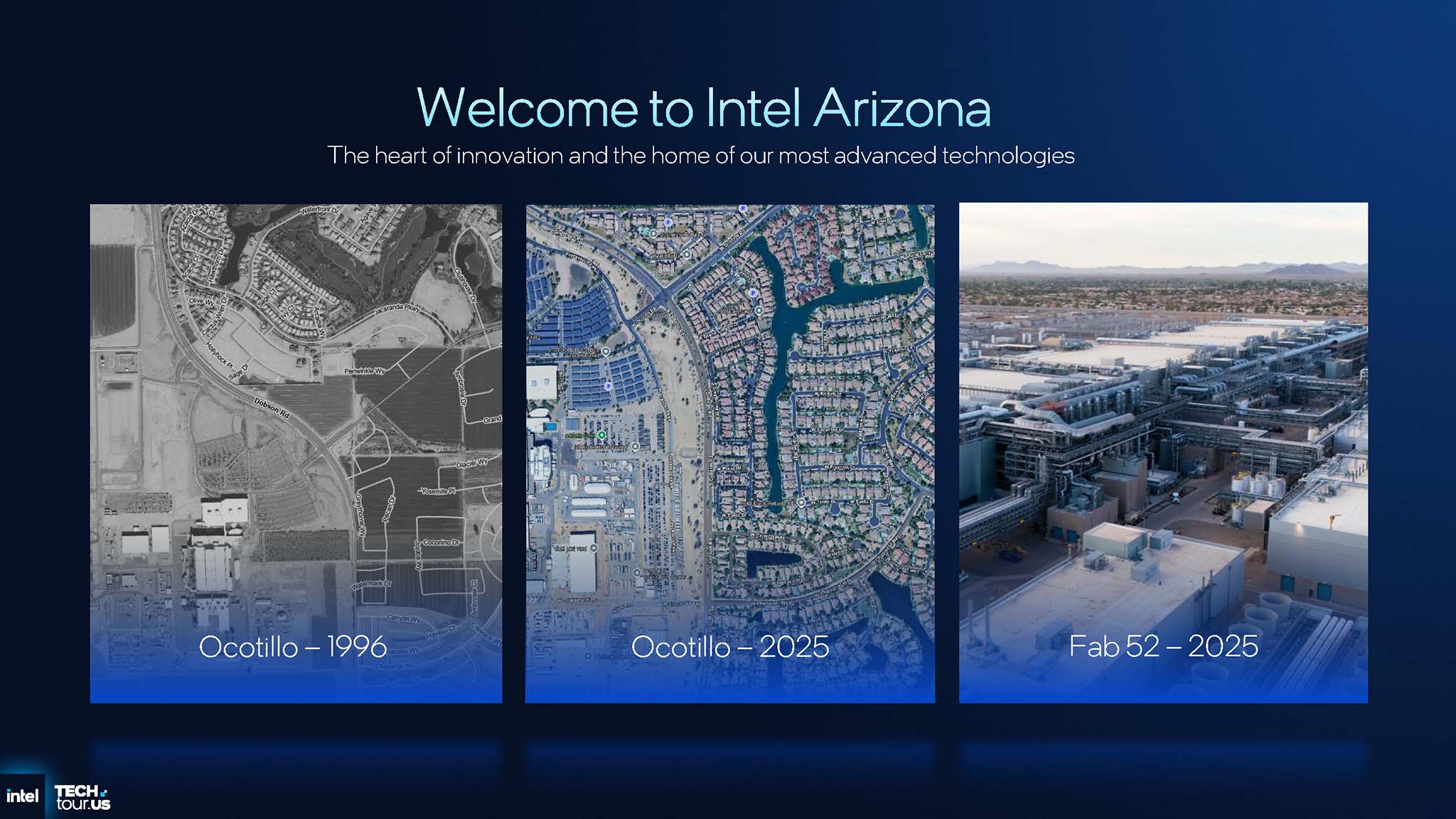
Intel has been in Arizona since 1979 and has accumulated investments of over $50 billion to date. The Ocotillo campus in Chandler, covering over 283 hectares, has become one of the most important semiconductor manufacturing centers in the world. Fab 52 is part of a $32 billion expansion plan in Arizona, along with Fab 62. The scale of Fab 52's construction is impressive, requiring five times the amount of structural steel as the Eiffel Tower and an automated material handling system (AMHS) of more than 30 miles with more than 2,100 autonomous vehicles.
Arizona is a desert environment, so the challenges are enormous for a semiconductor factory that requires a lot of clean water, but Intel has always put sustainability first. The entire Ocotillo site is powered by 100% renewable energy. In particular, Intel is pursuing a net positive water goal, with an on-site treatment facility capable of recycling more than 9 million gallons of water per day. These investments are not only socially responsible but also ensure the stability of production facilities worth tens of billions of dollars in the face of potential fluctuations in resources and environmental regulations.
Fab 52 has been officially operational since October 9, 2025. The factory is mass producing on the Intel 18A process, of which Panther Lake is one of the first products.


1 thought on “Intel Tech Tour 2025: The 18A era, reshaping AI strategy”